这首歌真是绝了。Whisper of Rain, 翻译过来叫雨的呢喃。76MB的无损Flac,记得带上Hifi耳机听。
另外,我最近领悟了一部绝世武功心法秘籍,那就是不带情绪地看问题、做事情。看问题突然就清晰了,逻辑突然就通畅了,把忍受变接受。
- What can defeat DISIRE?
- Biger DISIRE.
1 编程语言
1.1 硬件描述语言 HDL
VHDL, Verilog, SystemVerilog 基本都是从hdlbits这个刷题网站上学的。 硬件描述语言,并不是硬件设计语言,描述的意思是不能改变硬件的架构,只是描述它,将某一些部分连起来。
1.1.1 Verilog
可综合的意思是可以直接整合成电路。
a. 模块
1
2
3
4
module module_name (input a, input b, output y); // 括号里是端口列表
    // 定义信号和端口类型
    assign y = a & b; // 使用逻辑与操作
endmodule
b. 逻辑门
- AND
assign y = a & b,a、b都是0,y才是1.
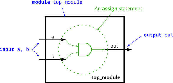
AND gate | 与门
- NOR
A NOR gate is an OR gate with its output inverted.
In Verilog, a NOR gate performs the logical NOT operation after an OR operation, meaning the output is true (1) only when all inputs are false (0). a、b都是1,y才是0.
assign y = ~(a | b)
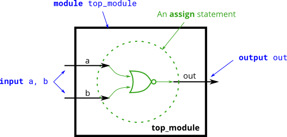
Nor gate | 或非门
- XOR 异或门
assign y = a ^ b,a、b只有1个是1(高电平),y才是1(高电平).
- XNOR
An XNOR gate, also known as an “equivalence gate,” outputs true (1) if the number of true inputs is even.
只有其中一项输入为高,输出为低;否则出高。
assign y = ~(a ^ b)

Xnor gate | 相等门
It first performs an XOR operation on a and b and then negates the result using the bitwise NOT operator (~). The XOR operation (^) results in true if the inputs are different and false if they are the same. The NOT operation then inverts this result, giving the XNOR behavior.
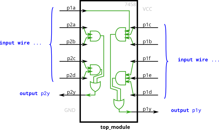
- 7458 chip
Xnor gate | 相等门
1
2
3
4
5
6
7
8
9
10
11
12
13
14
15
16
17
18
19
20
module top_module (
    input p1a, p1b, p1c, p1d, p1e, p1f,
    output p1y,
    input p2a, p2b, p2c, p2d,
    output p2y
);
    // Internal wires for intermediate signals
    wire im1, im2, im3, im4;

    // AOI gate logic for p2y
    assign im1 = p2a & p2b;
    assign im2 = p2c & p2d;
    assign p2y = im1 | im2;

    // AOI gate logic for p1y
    assign im3 = p1a & p1b & p1c;
    assign im4 = p1d & p1e & p1f;
    assign p1y = im3 | im4;

endmodule
也可以合并:
1
2
p2y = (p2a & p2b) | (p2c & p2d)
p1y = (p1a & p1b & p1c) | (p1d & p1e & p1f)
c. 数字
assign a = 3'b101;
3表示该数值是3位的。'b表示该数值是二进制(binary)格式。101是具体的二进制数值,对应的十进制值是5。
二进制前缀是 'b,八进制是 'o,十进制是 'd,而十六进制是 'h。
d. 端口
用于在模块(Module)之间传递信号(signal)
input:输入端口output:输出端口inout:双向端口
端口通常被声明为 wire 类型,特别需要存储值时使用 reg
1
2
3
4
5
module example_module (
    input  wire a,    // 输入端口
    output wire b,    // 输出端口
    inout  wire c     // 双向端口
);
e. 数据类型
- 信号(Signal)
- 信号 is also often called a driver that drives a value onto a wire.
- Describing signals as being driven (has a known value determined by something attached to it) or not driven by something。
wire:连续赋值- 信号线。不能存储值,仅用于连接和传递信号。
- 用作模块端口的类型,用于连接模块之间的信号。
- 还可以用于模块内部,连接不同的逻辑单元或用于组合逻辑的描述,连接模块内部的信号。
reg:用于存储值的变量,通常用于过程块。
f. 赋值语句
- 连续赋值:
assign语句用于持续地驱动wire类型的信号。assign只是把输入或者输出的wire连起来,所以顺序不重要1
assign y = a & b;
g. Vector
含义
vector表示多个位(bit)组成的信号。Vectors are used to group related signals using one name to make it more convenient to manipulate.
For example, wire [7:0] w; declares an 8-bit vector named w that is equivalent to having 8 separate wires.
打包数组(Packed Array):位宽(或维度)写在变量名称的前面。这些位是紧密地“打包”在一起的,这种表示在仿真器中有用,但在实际硬件实现中没有直接对应。
打包数组的定义格式/访问
1
type [msb:lsb] signal_name;
type:表示向量集合了哪些数据类型。msb:表示向量的最高位(most significant bit)的索引。lsb:表示向量的最低位(least significant bit)的索引。signal_name:向量的名称。
例如:
1
2
3
4
5
6
7
8
9
10
11
12
reg [7:0] data_byte; // 8位(8-elements)的寄存器,位索引范围是7到0。其中 8 位被打包在一起,形成一个单一的 8 位宽度的信号。
output reg [0:0] y;   // 1-bit reg that is also an output port (this is still a vector)
wire [0:15] data_word; // 16位的线(wire),位索引范围是0到15。

assign single_bit = data_byte[3]; // 获取data_byte的第4位(从0开始计数)

wire [3:0] lower_nibble;
assign lower_nibble = data_byte[3:0]; // 获取data_byte的低4位

wire [7:0] upper_byte, lower_byte;
wire [15:0] word;
assign word = {upper_byte, lower_byte}; // 将两个8位的byte连接成一个16位的word
向量的位数可以是任意整数,常用于表示数据的宽度,比如8位、16位或32位等。向量的 Type is ‘wire’ unless specified otherwise.
未打包数组(Unpacked Array):表示多个相同类型的元素的集合,每个元素本身可能是打包的。未打包数组的维度在变量名称后面指定。这种结构通常用于描述内存或寄存器文件等结构。
1
2
reg [7:0] mem [255:0]; // 256 个未打包元素,每个元素是一个 8 位打包向量。这个声明描述了一块内存,其中每个地址都存储一个 8 位的值。
`reg mem2 [28:0];      // 它有 29 个元素,每个元素都是一个 1 位的 reg 类型信号。这种表示方式在设计中非常常见,尤其是在需要表示多位数据存储结构时。
向量的方向 endianness
- 最左边的是 Most significant bit(MSB),最右边是 least significant bit。
- 向量最小的数,叫低位索引(lower index),比如
[0:15]里的0. - 向量有2种方向,一种是最右边的数大,最左边的数小,比如
[0:15],叫most significant bit has a lower index,也就是递增的,叫big-endian。反之就是little-endian。向量的方向一旦定义就不能改了,后面得一直怎么用,递增或者递减。
隐式网(implicit nets)
没有显式声明,但被编译器自动推断出来的信号。
- 使用
assign语句连接信号而没有显式声明信号类型时,Verilog会隐式创建一个网(通常是wire类型)。默认隐式网单比特宽度的。 - 将一个未声明的信号连接到模块端口,Verilog也会隐式创建一个网。
- `default_nettype none 禁用隐式网的自动创建。当该指令生效时,任何未声明的信号使用都会导致编译错误
- `default_nettype wire 恢复默认
操作符
- 逻辑操作符:
&、|、~ - 比较操作符:
==、!=、<、> - 算术操作符:
+、-、*、/
条件语句
if-else语句1 2 3 4 5
if (condition) begin // 真值条件下执行 end else begin // 否则执行 end
case语句1 2 3 4 5 6 7 8 9 10 11 12
case (变量) 值1: begin // 对应值1时执行 end 值2: begin // 对应值2时执行 end default: begin // 默认情况 end endcase end
always 和 initial 块
always:用于描述持续触发的行为,比如时钟敏感的行为。1 2 3
always @ (posedge clk) begin // 时钟上升沿时执行 end
initial:用于初始化操作,只执行一次。1 2 3
initial begin // 初始块中的代码 end
1.2 寄存器传输语言 RTL
写简单的测试平台。 硬件电路是并行执行的。
1.2.1 组合电路
1.2.2 时序电路
1.2.3 状态机
2. 开发工具/仿真工具
2.1 Vivado (Xilinx, By AMD)
2.1 Quartus (By Intel)
3 专业知识
数字电路,接口,计算机体系结构,信号处理